

If pc chips make the trendy world go round, then Nvidia and TSMC are flywheels holding it spinning. It’s price paying consideration when the previous says they’ve made a chipmaking breakthrough, and the latter confirms they’re about to place it into apply.
At Nvidia’s GTC developer convention this week, CEO Jensen Huang said Nvidia has developed software program to make a chipmaking step, known as inverse lithography, over 40 occasions quicker. A course of that often takes weeks can now be accomplished in a single day, and as an alternative of requiring some 40,000 CPU servers and 35 megawatts of energy, it ought to solely want 500 Nvidia DGX H100 GPU-based programs and 5 megawatts.
“With cuLitho, TSMC can cut back prototype cycle time, improve throughput and cut back the carbon footprint of their manufacturing, and put together for 2nm and past,” he mentioned.
Nvidia partnered with among the greatest names within the trade on the work. TSMC, the most important chip foundry on the earth, plans to qualify the strategy in manufacturing this summer time. In the meantime, chip designer, Synopsis, and tools maker, ASML, mentioned in a press release they are going to combine cuLitho into their chip design and lithography software program.
What Is Inverse Lithography?
To manufacture a contemporary pc chip, makers shine ultraviolet gentle by way of intricate “stencils” to etch billions of patterns—like wires and transistors—onto clean silicon wafers at near-atomic resolutions. This step, known as photolithography, is how each new chip design, from Nvidia to Apple to Intel, is manifested bodily in silicon.
The machines that make it occur, constructed by ASML, cost hundreds of millions of dollars and may produce near-flawless works of nanoscale artwork on chips. The top product, an instance of which is buzzing away close to your fingertips as you learn this, might be probably the most complicated commodity in historical past. (TSMC churns out a quintillion transistors every six months—for Apple alone.)
To make extra highly effective chips, with ever-more, ever-smaller transistors, engineers have needed to get artistic.
Do not forget that stencil talked about above? It’s the weirdest stencil you’ve ever seen. In the present day’s transistors are smaller than the wavelength of sunshine used to etch them. Chipmakers have to make use of some extraordinarily intelligent methods to design stencils—or technically, photomasks—that may bend gentle into interference patterns whose options are smaller than the sunshine’s wavelength and completely match the chip’s design.
Whereas photomasks as soon as had a extra one-to-one form—a rectangle projected a rectangle—they’ve essentially turn into increasingly sophisticated through the years. Essentially the most superior masks today are extra like mandalas than easy polygons.
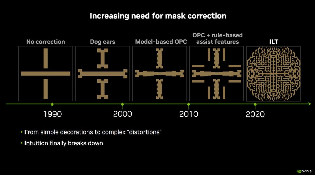
To design these superior photomask patterns, engineers reverse the method.
They begin with the design they need, then stuff it by way of a depraved mess of equations describing the physics concerned to design an appropriate sample. This step known as inverse lithography, and because the hole between gentle wavelength and have measurement has elevated, it’s turn into more and more essential to the entire course of. However because the complexity of photomasks will increase, so too does the computing energy, time, and price required to design them.
“Computational lithography is the most important computation workload in chip design and manufacturing, consuming tens of billions of CPU hours yearly,” Huang mentioned. “Huge knowledge facilities run 24/7 to create reticles utilized in lithography programs.”
Within the broader class of computational lithography—the strategies used to design photomasks—inverse lithography is likely one of the newer, extra superior approaches. Its benefits embrace larger depth of area and backbone and may profit the complete chip, however due its heavy computational raise, it’s at present solely used sparingly.
A Library in Parallel
Nvidia goals to scale back that raise by making the computation extra amenable to graphics processing items, or GPUs. These highly effective chips are used for duties with plenty of easy computations that may be accomplished in parallel, like video video games and machine studying. So it isn’t nearly operating present processes on GPUs, which solely yields a modest enchancment, however modifying these processes particularly for GPUs.
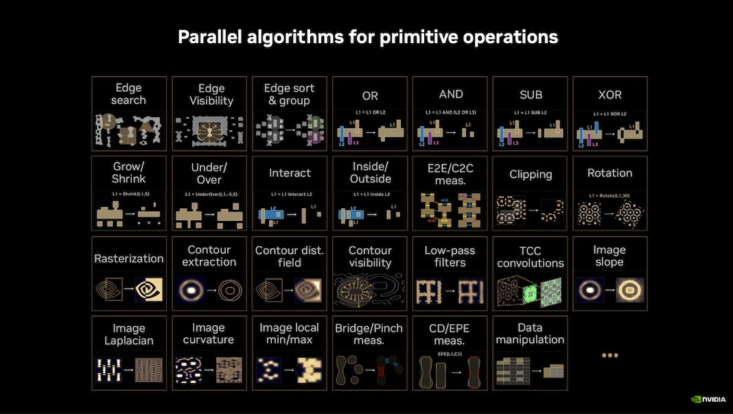
That’s what the brand new software program, cuLitho, is designed to do. The product, developed during the last 4 years, is a library of algorithms for the fundamental operations utilized in inverse lithography. By breaking inverse lithography down into these smaller, extra repetitive computations, the entire course of can now be break up and parallelized on GPUs. And that, based on Nvidia, considerably speeds every thing up.
“If [inverse lithography] was sped up 40x, would many extra individuals and firms use full-chip ILT on many extra layers? I’m certain of it,” mentioned Vivek Singh, VP of Nvidia’s Superior Expertise Group, in a talk at GTC.
With a speedier, much less computationally hungry course of, makers can extra quickly iterate on experimental designs, tweak present designs, make extra photomasks per day, and usually, broaden using inverse lithography to extra of the chip, he mentioned.
This final element is important. Wider use of inverse lithography ought to cut back print errors by sharpening the projected picture—that means chipmakers can churn out extra working chips per silicon wafer—and be exact sufficient to make options at 2 nanometers and past.
It seems making higher chips isn’t all concerning the {hardware}. Software program enhancements, like cuLitho or the elevated use of machine studying in design, can have a big effect too.
Picture Credit score: Nvidia